Noted:
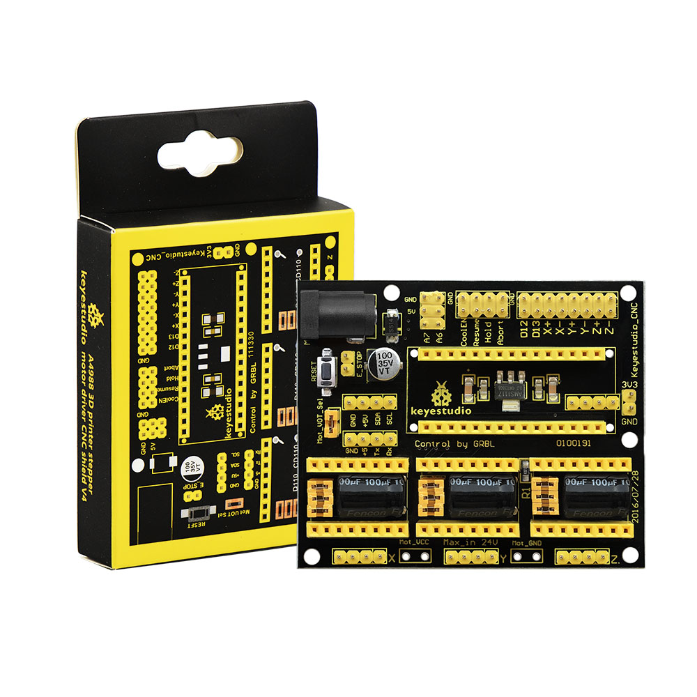
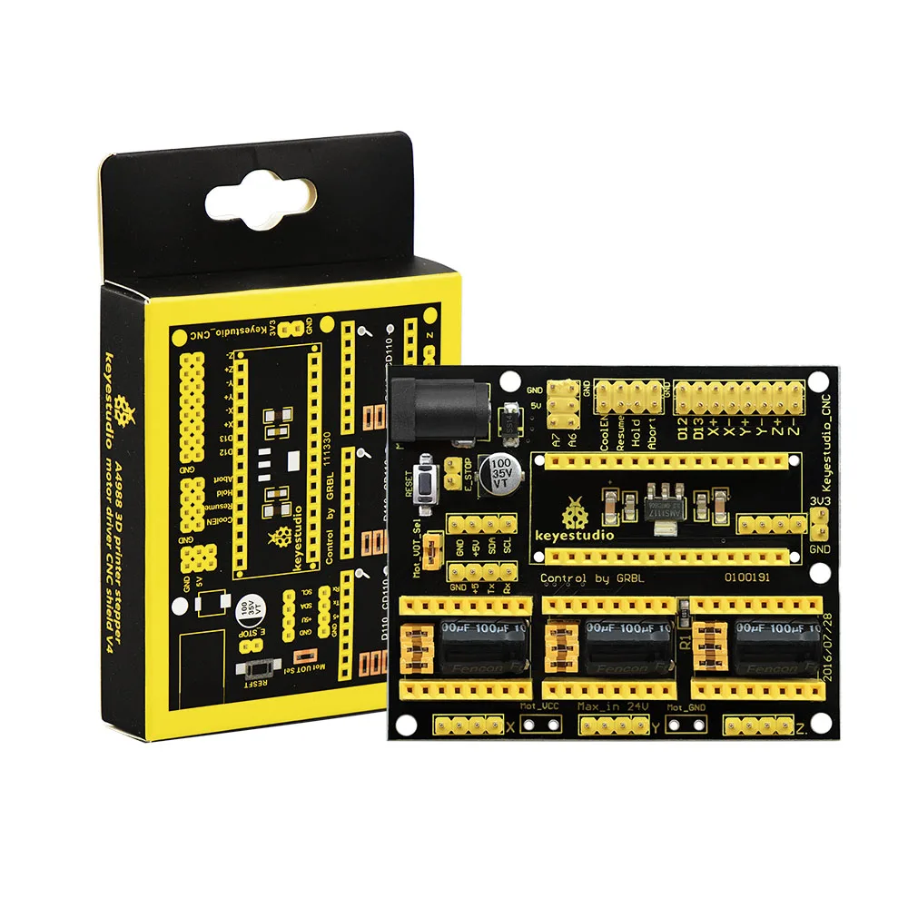
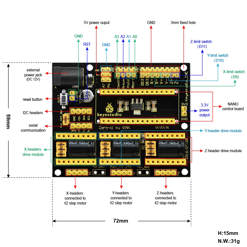
A. Corresponding interfaces of official web is shown as below:
#define X_STEP_BIT 2 // Uno Digital Pin 2
#define Y_STEP_BIT 3 // Uno Digital Pin 3
#define Z_STEP_BIT 4 // Uno Digital Pin 4
#define X_DIRECTION_BIT 5 // Uno Digital Pin 5
#define Y_DIRECTION_BIT 6 // Uno Digital Pin 6
#define Z_DIRECTION_BIT 7 // Uno Digital Pin 7
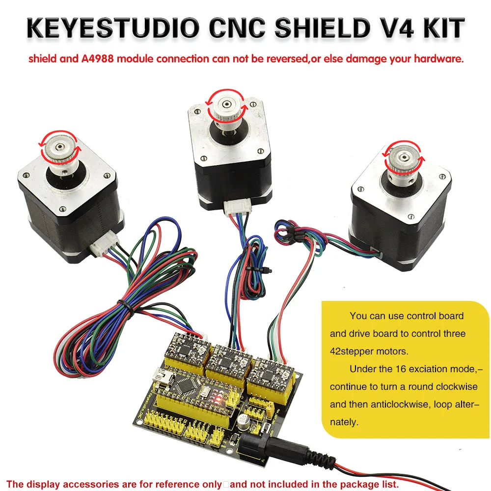
B.The product is equipped with A4988 driver module. If you want to change working mode, just need to adjust the level of ms1 ms2 ms3(DRV 8825 ms0 ms1 ms2) that have been connected to three pairs of pin header(with jumper cap). If plugging a jumper cap, the circuit is connected to GND. Namely, ms1 ms2 ms3(DRV 8825 ms0 ms1 ms2) are connected to GND, meaning the working mode has changed into full-step mode. The circuit is disconnected without jumper cap. If you want to connect the circuit with high level, you have to connect it to VCC by soldering.
The relation between working mode of A4988 module and MS1, MS2, MS3 is shown as below table:

The relation between working mode of DRV 8825 module and MS0, MS1, MS2 is shown as below table:


